As MediaCow Touch 2 enters yet another month of development and into its fourth year on March 2, 2025, I have been pushing more to work on the project. A reminder, however, real development started in June 2024.
System on Module
It appears I have not mentioned this before, but MediaCow Touch 2 is to use the Intel Processor N305 version of the LattePanda Mu. As of March 4, 2025, I do not have one one of these modules. I have held off from ordering one because no changes in the design have to be made to support the N305 version and I am currently unwilling to spend US$259 on the module given my ever limited funds.
A major difference between the N100 version and the N305 version is that the N305 version has a higher TDP that may have to be accounted for in power management and possibly cooling.
Side-mounted Display
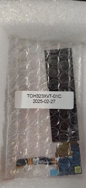
After I sent the payment on February 23, 2025 with an update about shipment being received on February 28, 2025. On March 3, 2025, I received the two TOH323XVT-01C AMOLED displays from Tailorpixels. I was amazed by how thin the displays were, practically as thin as paper.
The provider of the AMOLED display, Tailorpixels, has been greatly helpful with implementing the display into the project. The datasheet for the display has been updated twice since I have started working with the display, covering some things that I mentioned in my feedback. The latest revision of the datasheet was on March 3, 2025.
I am learning a lot about these displays while I am working with them, this being the first time I have looked into the MIPI-DSI interface in detail. One thing I noticed is that the display configuration would be done over the MIPI interface instead of with a separate SPI interface.
Side-mounted Display PCB
On February 20, 2025, I drew the schematic symbol for the GOWIN GW1N-UV2QN48C7/I6 FPGA. It was a tedious process though it was successful.
I was considering designing a board that connects to the Banana Pi F2P to test RGB-MIPI but not all of the RGB-capable pins on the SP7021 are exposed on the F2P's GPIO header, making this not possible to do with the Banana Pi BPI-F2P. Either I would have to go ahead and design the PCB for MediaCow Touch 2 or I design my own single board computer with the RGB pins exposed; Block-SP7021. Another alternative is to ask Sunplus for one of their development boards. I may go ahead and design Block-SP7021 since I already have mentioned that I would work on it at some point to help develop MediaCow Touch 2.
Though the PCB does not necessarily have to be tested with the SP7021, I'd like to ensure that this configuration would work with the SP7021.
On February 24, 2025, after successfully drawing the schematic symbol for the FPGA, I started the schematic for the side-mounted display. The input would have the same pinout as various displays from Adafruit. Block-SP7021 would use the same pinout to reflect this.
I realize that using an FPGA to achieve this is no simple feat, especially that implementing a MIPI transmitter block is required. There are no easier or lower-cost alternatives to this, that I know of, so I must go on. I always wanted to do something with an FPGA anyway...
On February 28, 2025, I ran into a potential problem with the FPGA where some of the pins that are used for display data may also have to be used for programming the FPGA. Unlike many other IC datasheets, GOWIN's documentation has topics per document where the documents cover the entire series. This may be more convient in some ways though I have found it confusing at times.
With support from GOWIN and reading through documents UG171-1.8E and DS100. I determined that Bank 3 would be used for the MIPI transmitter. With the display using a single-lane interface, two differential pairs are needed.
The Design
I started the design for the side-mounted display PCB on February 24, 2025 though I started to make progress on it starting March 2.
I looked over the pinout of the display. I noticed that the display uses multiple voltages for IO and power. Most IO seems to use 1.8v, the PMIC enable signal is 3.3v, the PMIC input voltage can anything within 2.9v to 5.0v and the touchscreen supply is 2.8v.
Any 1.8v IO signals may have to be shifted to 3.3v to be used with the SP7021.
There are pins for a second MIPI lane on the connector, they are unused for this display and are labeled as NC in the datasheet.
I noticed there is a TE pin that is the Tearing Effect signal. A question about this was asked on the STMicroelectronics Community forum, mentioning another display from Tailorpixels. Supposedly this pin is used to prevent the display from being updated while data is being written to the controller's framebuffer. I may have this pin connected to a free pin on the FPGA.
Display Adapter PCB
On February 23, 2025, I continued the design for the display adapter PCB that connects the Innolux N140JCN-GS9 (and other 40-pin 2-lane eDP + touch displays) to the LattePanda Mu.
I left some special features on the PCB: for one, the PCB has connectors for both I2C and USB to support panels with either an USB or I2C interface. Another is that the PCB has solder jumpers that give the option to have the backlight controlled by the LattePanda Mu or external signals. The latter is important since it would have SMEC be able to control the backlight or for debugging purposes, have the LattePanda Mu control the backlight.
I considered switching out the 40-pin IPEX connector for a 30-pin connector then use the adapater cable that came with the DFRobot display. However, I decided to keep the 40-pin connector to minimize the amount of unique parts as both sides can use the same connector.